Die-Cut Polyimide Tape for IC Packaging – Precision & Protection
Share
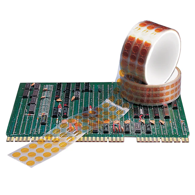
Die-cut polyimide tape (also known as Kapton tape) is a high-performance, heat-resistant adhesive material that has been precision-cut into custom shapes for specialized applications in semiconductor packaging and IC manufacturing. With its exceptional thermal stability (up to 260°C), electrical insulation, and chemical resistance, it plays a vital role in protecting delicate components during wire bonding, encapsulation, and thermal processing.
In IC packaging, die-cut polyimide tape is used for:
✔ Wafer dicing protection – Shields silicon wafers from contamination during cutting.
✔ Wire bonding isolation – Prevents short circuits between fine-pitch bond wires.
✔ Encapsulation masking – Defines precise areas for epoxy molding compounds (EMC).
✔ Lid attach & heat spreader bonding** – Ensures secure thermal interface material (TIM) application.
Key Benefits of Die-Cut Polyimide Tape in IC Packaging
1️⃣ Extreme Heat Resistance for High-Temp Processes
- Withstands **260°C+ temperatures, making it ideal for lead-free soldering, curing, and reflow processes.
- Unlike PVC or PET tapes, it won’t melt or leave residue, ensuring clean post-processing removal.
2️⃣ Precision Die-Cutting for Miniaturized IC Designs
- Laser-cut into exact shapes (gaskets, frames, spacers) for tight-tolerance packaging needs.
- Critical for fan-out wafer-level packaging (FOWLP) and 3D IC stacking.
3️⃣ Superior Electrical Insulation & ESD Protection
- Low-static properties prevent electrostatic discharge (ESD) damage to sensitive ICs.
- Dielectric strength (5,000V+) isolates high-voltage components in power ICs.
4️⃣ Chemical & Moisture Resistance for Reliability
- Resists flux, solvents, and cleaning agents used in post-packaging processes.
- Unlike paper tapes, it won’t absorb moisture, preventing corrosion in humid environments.
---
Top Applications in IC Packaging
✔ Wafer Backside Protection – Guards against scratches during grinding and handling.
✔ BGA & CSP Substrate Masking – Defines solder ball placement areas.
✔ EMC Dam Formation – Creates barriers for precise epoxy encapsulation.
✔ Thermal Interface Bonding – Secures heat spreaders in advanced packaging.
- "Best die-cut polyimide tape for IC packaging"
- "Kapton tape vs PET for semiconductor masking"
- "How to use precision-cut tape in wafer dicing"
- "High-temp adhesive solutions for 3D IC stacking"
- "Where to buy custom die-cut Kapton tape"